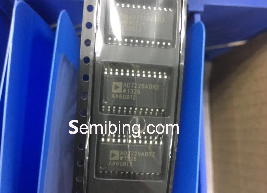
Part Number AD7228ABRZ-ND
Manufacturer Analog Devices Inc.
Manufacturer Part Number AD7228ABRZ
Description IC DAC 8BIT V-OUT 24SOIC
Manufacturer Standard Lead Time 8 Weeks
Detailed Description 8 Bit Digital to Analog Converter 8 24-SOIC
Datasheets AD7228A
Product Training Modules Data Converter Fundamentals
DAC Architectures
Five Things to Know About DACs Part 1: Resolution vs. Accuracy
Five Things to Know About DACs Part 2: Total Unadjusted Error (TUE)
Five Things to Know About DACs Part 5: Dynamic Performance
View More
Video File High-Speed Converters by Analog Devices
Design Resources Development Tool Selector
Featured Product Analog Devices IoT and the Intelligence of Things
Interactive RF Signal Chain
EDA / CAD Models AD7228ABRZ by SnapEDA
EDA / CAD Models Download from Ultra Librarian
Online Catalog 8 Bit
Product Attributes
TYPE DESCRIPTION SELECT ALL
Categories Integrated Circuits (ICs)
Data Acquisition – Digital to Analog Converters (DAC)
Manufacturer Analog Devices Inc.
Series –
Packaging Tube
Part Status Active
Number of Bits 8
Number of D/A Converters 8
Settling Time 5µs, 7µs
Output Type Voltage – Buffered
Differential Output No
Data Interface Parallel
Reference Type External
Voltage – Supply, Analog 10.8V ~ 16.5V, ±5V
Voltage – Supply, Digital 13.5V ~ 16.5V
INL/DNL (LSB) ±1 (Max), ±1 (Max)
Architecture R-2R
Operating Temperature -40°C ~ 85°C
Package / Case 24-SOIC (0.295″, 7.50mm Width)
Supplier Device Package 24-SOIC
Mounting Type Surface Mount
Base Part Number AD7228
GENERAL GENERAL DESCRIPTION The AD7228 contains eight 8-bit voltage mode digital-to- analog converters (DACs), with output buffer amplifiers and interface logic on a single monolithic chip. No external trims are required to achieve the full specified performance for the device. Separate on-chip latches are provided for each of the eight DACs. Data is transferred into the data latches through a common 8-bit, TTL/CMOS-compatible input port (5 V). The A0, A1, and A2 address inputs determine which latch is loaded when WR goes low. The control logic is speed compatible with most 8-bit microprocessors. Specified performance is guaranteed for input reference voltages from 2 V to 10 V when using dual supplies. The device is also specified for single-supply operation using a reference of 10 V. Each output buffer amplifier is capable of developing 10 V across a 2 kΩ load. The AD7228 is fabricated on an all ion implanted, high speed, linear-compatible CMOS (LC2 MOS) process, specifically developed to integrate high speed digital logic circuits and precision analog circuits on the same chip. PRODUCT HIGHLIGHTS 1. The single chip design of eight 8-bit DACs and amplifiers allows a dramatic reduction in board space requirements and offers increased reliability in systems using multiple converters. The PDIP, CERDIP, and SOIC pinout is aimed at optimizing board layout with all analog inputs and outputs at one side of the package and all digital inputs at the other. 2. The voltage mode configuration of the DACs allows single supply operation of the AD7228. The device can also be operated with dual supplies giving enhanced performance for some parameters. 3. The AD7228 has a common 8-bit data bus with individual DAC latches, providing a versatile control architecture for simple interface to microprocessors. All latch enable signals are level triggered and speed compatible with most high performance 8-bit microprocessors. DESCRIPTION The AD7228 contains eight 8-bit voltage mode digital-to- analog converters (DACs), with output buffer amplifiers and interface logic on a single monolithic chip. No external trims are required to achieve the full specified performance for the device. Separate on-chip latches are provided for each of the eight DACs. Data is transferred into the data latches through a common 8-bit, TTL/CMOS-compatible input port (5 V). The A0, A1, and A2 address inputs determine which latch is loaded when WR goes low. The control logic is speed compatible with most 8-bit microprocessors. Specified performance is guaranteed for input reference voltages from 2 V to 10 V when using dual supplies. The device is also specified for single-supply operation using a reference of 10 V. Each output buffer amplifier is capable of developing 10 V across a 2 kΩ load. The AD7228 is fabricated on an all ion implanted, high speed, linear-compatible CMOS (LC2 MOS) process, specifically developed to integrate high speed digital logic circuits and precision analog circuits on the same chip. PRODUCT HIGHLIGHTS 1. The single chip design of eight 8-bit DACs and amplifiers allows a dramatic reduction in board space requirements and offers increased reliability in systems using multiple converters. The PDIP, CERDIP, and SOIC pinout is aimed at optimizing board layout with all analog inputs and outputs at one side of the package and all digital inputs at the other. 2. The voltage mode configuration of the DACs allows single-supply operation of the AD7228. The device can also be operated with dual supplies giving an enhanced performance for some parameters. 3. The AD7228 has a common 8-bit data bus with individual DAC latches, providing a versatile control architecture for a simple interface to microprocessors. All latch enable signals are level triggered and speed compatible with most high-performance 8-bit microprocessors.
